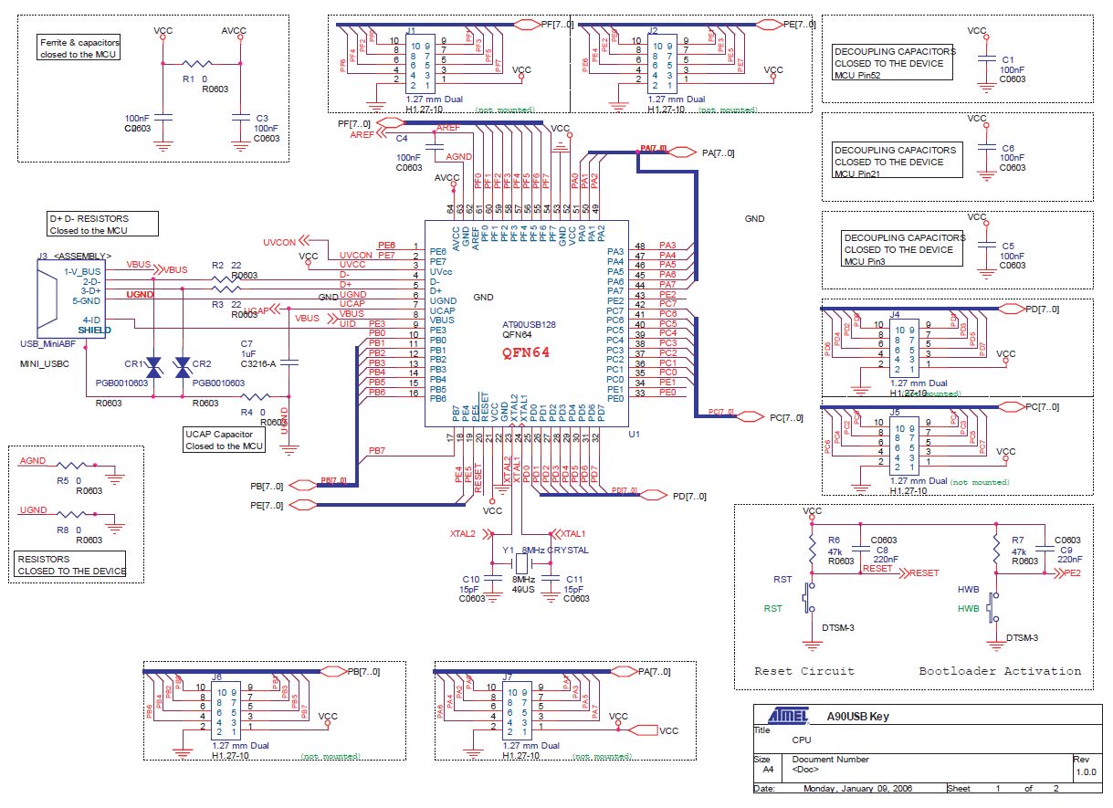
(shorthand: Port x, Pin y = Pxy)
USB
  D- -
  D+ -
  UGND -
  VBUS -
  PE3 -
Joystick (4+1 directions) - NB uses pins from 2 ports
  PB5 - Select (centre button)
  PB6 - Left
  PB7 - Up
  PE4 - Right
  PE5 - Down
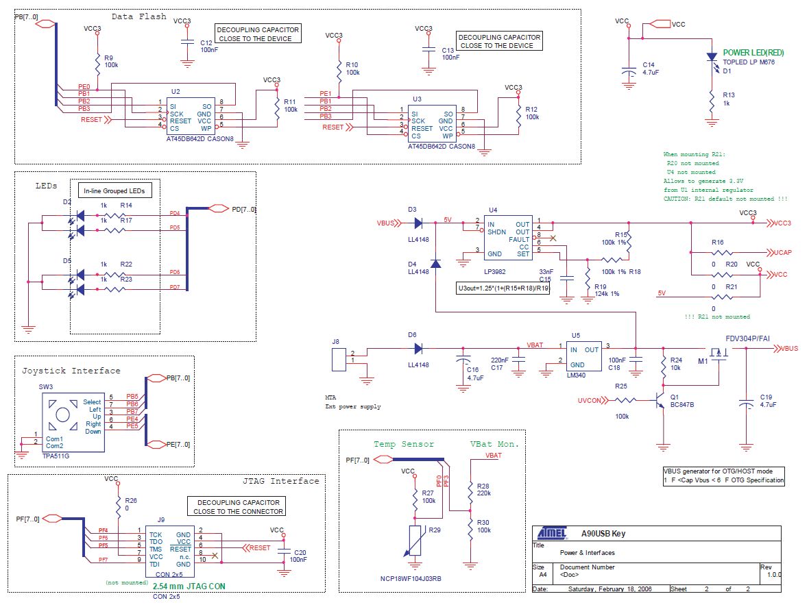
LEDs (2 bicolor)
  PD4 - LED D2 Red
  PD5 - LED D2 Green
  PD6 - LED D5 Green
  PD7 - LED D5 Red
Temperature Sensor
PF0 - thermistor R29
DataFlash Memory
   Two (U2 and U3) 64-megabit Serial Interface Flash memories (AT45DB642D, CASON8 package) connected
     to the AT90USB Serial Port Interface (SPI).

   Chip1 (U2)
   PE0 - U2 pin 4 - Chip Select signal
   PB1 - U2 pin 2 - SCK - Serial Clock
   PB2 - U2 pin 1 - SI - Serial Input
   PB3 - U2 pin 4 - SO - Serial Output

   Chip2 (U3)
   PE1 - U3 pin 4 - Chip Select signal
   PB1 - U3 pin 2 - SCK - Serial Clock
   PB2 - U3 pin 1 - SI - Serial Input
   PB3 - U3 pin 4 - SO - Serial Output

DataFlash Pins
   1. SI - Serial Input: The SI pin is used to shift data into the device.
      The SI pin is used for all data input including command and address sequences.
      Data on the SI pin is always latched on the RISING edge of SCK.
   2. SCK - Serial Clock: External signal used to control the flow of data to and from the device.
      Inputs are latched on the rising edge, while output on the falling edge of SCK/CLK.
   3. RESET - Reset: A low state will terminate all operations and reset the internal state machine to idle.
      Work will resume when the RESET pin is brought back to a high level.
   4. CS - Chip Select: Asserting the CS pin selects the device.
      When deasserted, the device will normally be placed in the standby mode (not Deep Power-Down mode),
      output pin goes into a high-impedance state, data will not be accepted on the input pin.
   5. WP - Write Protect: This pin is hardwired high on the key. Usually When WP pin is asserted,
      all sectors specified for protection by the Sector Protection Register will be protected against
      program and erase operations regardless of whether the Enable Sector Protection command has been issued or not.
   6. VCC - Device Power Supply: The VCC pin is connected to system Vcc.
   7. GND - Ground: The ground reference for the power supply (connected to the system ground)
   8. SO - Serial Output: The SO pin is used to shift data out from the device.
      Data on the SO pin is always clocked out on the FALLING edge of SCK.
AT90USB1287 Chip Pin Connections (with on-board functions)
1 – PE6 = User port (not mounted)
2 – PE7 = UVCON
3 – UVcc = VCC - ferrite and capacitors (closed to MCU)
4 – D- = D- on USB MiniABF
5 – D+ = D+ on USB MiniABF
6 - UGND = D- on USB MiniABF; Resistor closed to device
7 – UCAP – Capacitor (closed to MCU)
8 - VBUS= VBUS on USB MiniABF
9 – PE3 = User port (not mounted); ID on USB MiniABF
10 – PB0 = User port (not mounted)
11 – PB1 = User port (not mounted); Data Flash – U2 SI; Data Flash – U3 SI
12 – PB2 = User port (not mounted); Data Flash – U2 SCK; Data Flash – U3 SCK
13 – PB3 = User port (not mounted); Data Flash – U2 SO; Data Flash – U3 SO
14 – PB4 = User port (not mounted)
15 – PB5 = User port (not mounted) ; Joystick Interface – Select Button
16 – PB6 = User port (not mounted) ; Joystick Interface – Left Button
17 – PB7 = User port (not mounted); Joystick Interface – Up Button
18 – PE4 = User port (not mounted);; Joystick Interface – Right Button
19 – PE5 = User port (not mounted);; Joystick Interface – Down Button
20 – RESET = Reset Button (Warm-Reset [the board also resets the chip on power-on])
21 – VCC = ferrite and capacitors (closed to MCU)
22 - GND
23 – XTAL2 – 8MHz crystal
24 – XTAL1 – 8MHz crystal
25 – PD0 = User port (not mounted)
26 – PD1 = User port (not mounted)
27 – PD2 = User port (not mounted)
28 – PD3 = User port (not mounted)
29 – PD4 = User port (not mounted); In-line Grouped LEDs – D2 Red
30 – PD5 = User port (not mounted) ; In-line Grouped LEDs – D2 Green
31 – PD6 = User port (not mounted) ; In-line Grouped LEDs – D5 Green
32 – PD7 = User port (not mounted) ; In-line Grouped LEDs – D5 Red
33 – PE0 = User port (not mounted); Data Flash – U2 CS (Select)
34 – PE1 = User port (not mounted); Data Flash – U3 CS (Select)
35 – PC0 = User port (not mounted)
36 – PC1 = User port (not mounted)
37 – PC2 = User port (not mounted)
38 – PC3 = User port (not mounted)
39 – PC4 = User port (not mounted)
40 – PC5 = User port (not mounted)
41 – PC6 = User port (not mounted)
42 – PC7 = User port (not mounted)
43 – PE2 = User port (not mounted); HWB button (runs bootloader if pressed while reset button is released)
44 – PA7 = User port (not mounted); AD7 - ADC multiplexed with other port A pins (10bit resolution)
45 – PA6 = User port (not mounted); AD6 - ADC multiplexed with other port A pins (10bit res)
46 – PA5 = User port (not mounted); AD5 - ADC multiplexed with other port A pins (10bit res)
47 – PA4 = User port (not mounted); AD4 - ADC multiplexed with other port A pins (10bit res)
48 – PA3 = User port (not mounted); AD3 - ADC multiplexed with other port A pins (10bit res)
49 – PA2 = User port (not mounted); AD2 - ADC multiplexed with other port A pins (10bit res)
50 – PA1 = User port (not mounted); AD1 - ADC multiplexed with other port A pins (10bit res)
51 – PA0 = User port (not mounted); AD0 - ADC multiplexed with other port A pins (10bit res)
52 - VCC = ferrite and capacitors (closed to MCU)
53 - GND
54 – PF7 = User port (not mounted) ; JTAG Interface - TDI; ADC7
55 – PF6 = User port (not mounted) ; JTAG Interface - TDO; ADC6
56 – PF5 = User port (not mounted) ; JTAG Interface - TMS; ADC5
57 – PF4 = User port (not mounted); JTAG Interface - TCK; ADC4
58 – PF3 = User port (not mounted); Battery Voltage Monitor; ADC3 - with gain of 1x, 10x (8 bit resolution), or 200x (7 bit res)
59 – PF2 = User port (not mounted); ADC2 - with gain of 1x, 10x (8 bit resolution), or 200x (7 bit res)
60 – PF1 = User port (not mounted); ADC1 - with gain of 1x, 10x (8 bit resolution), or 200x (7 bit res)
61 – PF0 = User port (not mounted); Temp Sensor (thermistor); ADC0 - with gain of 1x, 10x (8 bit resolution), or 200x (7 bit res)
62 - AREF
63 – AGND = Resistor closed to device
64 - AVCC = ferrite and capacitors (closed to MCU)
回路図